


The integration of optical communication and signal processing functionalities as part of silicon integrated circuits, or silicon photonics, is widely regarded as key enabling technology for the future growth of data networks. Our group designs, fabricates and characterizes silicon photonic devices regularly. We rely on in-house, quick-turnaround fabrication within Micro-Nano Fabrication Unit (MNFU) of the Faculty of Electrical and Computer Engineering of the Technion, as well as on collaboration with the several industrial foundries in Israel and worldwide.
Specific projects include:
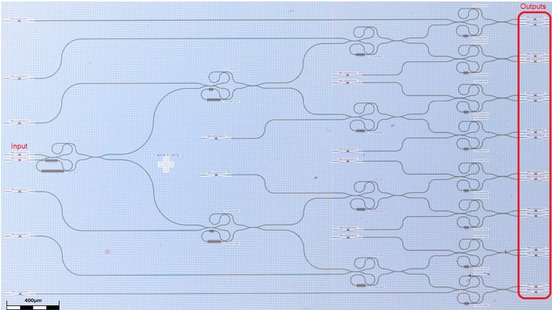 Wavelength-division multiplexing (WDM) of optical communication data channels on a silicon photonic chip. Devices supporting up to 16 channels have been fabricated and tested, operating at 1310 nm and 1550 nm wavelengths. The devices rely on multiple Mach-Zehnder interferometers, cascaded in a tree topology. To improve the response and transfer functions of multiplexer elements, feedback paths in the form of ring resonators are embedded within the devices layout. We rely on synthesis concepts rooted in digital signal processing for the design of complex, high-performance filters.
The transfer functions of photonic circuits can be modified and adjusted through the application of control currents to local heating elements. We have designed and employed universal filter stages, whose response can be broadly tuned over a range of target shapes. Recently, we combined a tunable filter stage alongside a detector on the chip, to obtain in integrated spectrum analyzer device with GHz-scale resolution.
 Surface acoustic waves (SAWs) – photonic devices in silicon. Analog signal processing of information-carrying waveforms requires long temporal delays, which cannot be accommodated in optical waveguides due to excessive footprint and losses. To work around this difficulty, information may be converted to the form of slow-moving surface acoustic waves (SAWs). The concept is widely employed in analog electronics for decades, and it relies on piezo-electric transduction to transfer information between electronics and acoustics. Silicon, however, is non-piezo-electric.
Our group has introduced a concept of SAW-photonic devices in standard silicon-on-insulator. Piezo-electric transduction and detection are replaced by the absorption of one modulated optical carrier in metal, and the photo-elastic modulation of another in a standard waveguide, respectively. Delays as long as 175 ns are acquired within 660 microns length. A similar delay in a silicon-photonic waveguide would require 17.5 meters, with losses above 1,000 dB. The concept is used in integrated, discrete-time microwave-photonic filters, microwave-frequency oscillators, and analysis of the elastic properties of deposited thin layers.